Power semiconductors for control, regulation, and switching purposes require higher voltages and greater currents. The switching action of the power semiconductor is controlled by the charge and discharge of the gate capacitance. The charge and discharge of the gate capacitance is usually controlled by the gate resistance. By using a typical +15V control voltage (VG(on)), the IGBT is turned on, and when the negative output voltage is -5 ... -8...-15V, the IGBT is turned off. The dynamic performance of the IGBT can be adjusted by the gate resistance value. The gate resistance affects the switching time, switching losses, and various other parameters of the IGBT, from electromagnetic interference EMI to voltage and current rate of change. Therefore, the gate resistance must be carefully selected and optimized according to the parameters of the specific application.
The setting of each IGBT switching characteristic can be affected by the external resistance RG. Since the input capacitance of the IGBT changes during switching, it must be charged and discharged. The gate resistor determines the charge and discharge by limiting the amplitude of the gate current (IG) pulse during turn-on and turn-off (see Figure 1). . As the peak current of the gate increases, the turn-on and turn-off times will be shortened and the switching losses will also be reduced. Reducing the resistance of RG(on) and RG(off) increases the gate peak current. When reducing the resistance of the gate resistance, it is necessary to consider the current variation characteristic di/dt generated when a large current is switched too fast. Stray inductance in the circuit creates large voltage spikes on the IGBT. This effect can be observed in the waveform diagram when the IGBT shown in Fig. 2 is turned off. The shaded portion of the figure shows the relative value of the turn-off loss. An instantaneous voltage spike on the collector-emitter voltage can damage the IGBT, especially in the case of a short-circuit shutdown operation, since the di/dt is large. Vstray can be reduced by increasing the value of the gate resistance. Therefore, the risk of IGBT damage due to overvoltage is eliminated. Fast turn-on and turn-off will result in higher dv/dt and di/dt, respectively, which will result in more electromagnetic interference (EMI), which can cause circuit failure. Table 1 shows the effect of different gate resistance values ​​on di/dt.

Figure 1 conduction, shutdown / gate current
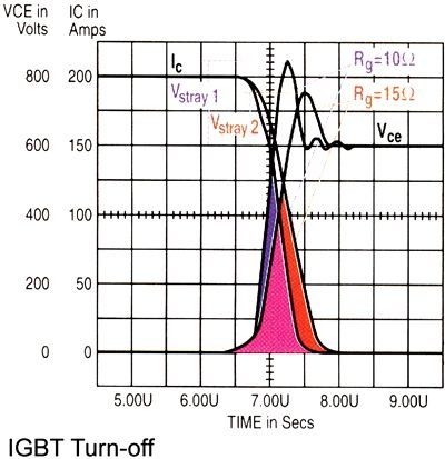
Figure 2 IGBT off
Table 1 Rate of change / characteristics
Rating/ Characteristics | R G ì | R G î |
T on | ì | î |
T off | ì | î |
E on | ì | î |
E off | ì | î |
Turn-on peak current | î | ì |
Turn-off peak current diode | î | ì |
Dv/dt | î | ì |
Di/dt | î | ì |
Voltage spike | î | ì |
EMI noise | î | ì |
Multi layer PC sheet is used for embossed carrier tape helping protect and transport electrostatically-sensitive electrical and electronic devices,the width can be from 8mm~88mm.Our Strengthen product is PC balck conductive sheet.
1.Descriptions
1. Width: 200mm~750mm (Tolerance: ± 1mm) ;
2. Thickness: 0.2mm~1.0mm (Tolerance: ± 0.02mm) ;
3. Length is customized. it can be jumbo roll,slitted roll
4. Density:1.20g/cm3
5. Color: black,
5. Surface resistivity:10e4~10e6
6. Process:Monolayer 3 layers co-extrustion
7. One side is glossy another side is matte
8. Certificates: : ISO9001,REACH,CTI RoHS.
2.Features
*Available in custom width and thickness within 0.2mm to 1.0mm
* No dependency on humidity.
*Stable surface resistivity
*Excellent dimensional stability for deep-drawing or precision forming.
*Thickness tolerence within 5%.
*Eecellent bending strength
*Good low temperature toughness
*Less Burrs and fines
*Good compatibility with different kinds of Cover Tape
PC Sheet For Carrier Tape,PC Black Conductive For Carrier Tape,Polycarbonate Carrier Tape Material,PC Black Conductive
Pujiang Yitong Plastic Electronic Co., Ltd. , http://www.yitongplastic.com