The application of solar photovoltaic systems is becoming more and more extensive. In particular, mobile systems benefit from solar energy without spending a penny. At the same time, due to the rising cost of conventional electricity, solar energy has great appeal for home applications. The energy efficiency of the solar cells themselves and the solar inverters connecting the solar cells to the public grid or distributed power sources are the key to the success of this technology. Today, advanced solar inverters with a maximum output of 5 kW have a two-level topology.
Each group is connected to its own power regulator and then connected to the common DC bus. Power conditioners enable solar cells to operate at maximum efficiency. Solar inverters can generate AC voltages that feed the mains. Please note that the power supply network is a dummy circuit that can be used for any inverter topology, plus a mains transformer and an output filter that prevents the DC component from entering the mains.
However, there are systems that do not use transformers, depending on the legal background of the country in which the solar inverter is sold. The purpose of allowing countries that do not use transformers is to increase system efficiency because transformers result in a 1 to 2 percentage point drop in efficiency. On the other hand, the inverter must avoid the direct current component and require a current of less than 5mA. Although this is difficult to achieve, we have succeeded in achieving higher efficiency. Table 1 shows the contribution of each stage to the system loss, system size, and system cost.
It is easy to see that transformers are major contributors to system losses and costs. However, transformers must be used in many countries, so it is not within the consideration of reducing losses. The output filter attenuates the current ripple generated by the output inverter stage. The size and cost of this filter is inversely proportional to the inverter switching frequency. The higher the switching frequency, the smaller the filter size and the cheaper the price. However, this relationship creates a tradeoff between the switching frequency and the switching losses in the hard-switched state—the higher the switching frequency, the greater the loss, and the lower the efficiency. From 16kHz to 20kHz switching frequency, due to lower audio noise and higher efficiency, it can meet the requirements of solar inverters. Therefore, the power circuit has yet to be further studied.
The following will compare the advantages of several semiconductor technologies that apply to these two levels.
Power semiconductors for DC/AC boost converters
The DC/DC converter is operated at a switching frequency of 100 kHz or above. The converter operates in continuous mode, which means that the current in the boost inductor produces a continuous waveform at nominal conditions. When the transistor is turned off and the diode is used as a freewheeling diode, the transistor can charge the inductor. This means that when the transistor is turned back on, the diode can be actively turned off. The following figure shows the typical reverse recovery characteristics of a typical silicon diode (black and red curves in Figure 2).
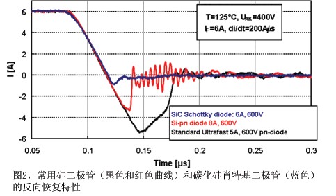
The reverse recovery characteristics of silicon diodes result in higher losses in boost transistors and corresponding diodes. Silicon carbide diodes do not have this problem (as shown by the blue curve in Figure 2). It is only due to the capacitive nature of the diode that produces an instantaneous negative current, which is caused by the junction capacitance of the diode. Silicon carbide diodes can greatly reduce transistor turn-on losses and turn-off losses of diodes, and can also reduce electromagnetic interference because the waveform is very smooth and there is no oscillation.
Many processes have been reported in the past to avoid loss caused by the diode's reverse recovery characteristics, such as zero-current-switching zero-current switching. All of these will greatly increase the number of components and the complexity of the system. The result is often a decrease in stability. It is particularly worth mentioning that even with a hard-switched Schottky diode using silicon carbide, the same efficiency can be achieved with a minimum number of components.
High switching frequency also requires high performance boost transistors. The introduction of super-junction transistors (such as CoolMOS) brings hope for further reducing the MOSFET's on-resistance per unit area RDS(on), as shown in Figure 3.
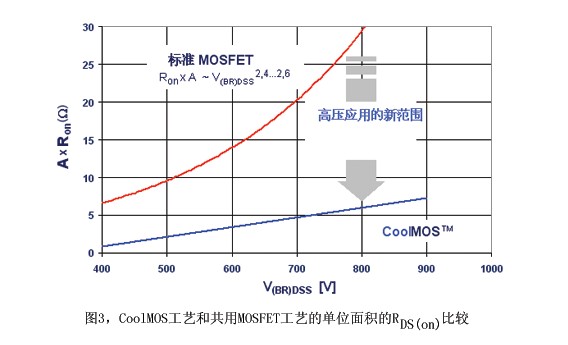
It is easy to see that the RDS(on) per unit area is about 4 to 5 times lower than the CoolMOS compared to the standard process. This means that CoolMOS achieves the lowest absolute on-resistance value in a standard package. This will result in the lowest conduction loss and highest efficiency. The RDS(on) per unit area of ​​the CoolMOS process shows better linearity. When the voltage is 600V, the advantage of CoolMOS is obvious, if the voltage is higher, its advantage will be strengthened. At present, the highest voltage level is 800V.
After several studies have shown that: the use of silicon carbide diodes and super-junction MOSFETs such as CoolMOS, is superior to the standard MOSFET and diode technology (shown in Figure 4) solution.

Power semiconductors for inverters
The output inverter connects the DC bus and the grid. In general, the switching frequency is not as high as the DC/DC converter. The output converter must handle the sum of the currents produced by all the group converters. Insulated gate bipolar transistors (IGBTs) are ideal devices for use in this inverter. Figure 5 shows two cross-sections of the IGBT process.
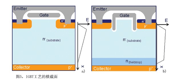
Both processes use a wafer thinning process designed to reduce conduction losses and switching losses caused by too large substrate thickness. The standard process and the TrenchStop process are non-epitaxial IGBT processes. The transistor growth process is not used because the cost of such processes is high because the blocking voltage is determined by the thickness of the growing crystal.
In the off state, the standard NPT cell forms a triangular electric field inside the semiconductor. All blocking voltages are covered by the n area of ​​the substrate
The absorption (depending on its thickness) is such that the electric field drops to 0 before entering the collector region. The thickness of the 600V chip is 120mm and the thickness of the 1200V chip is 170mm. The saturation voltage is a positive temperature coefficient, which simplifies parallel use.
The TrenchStop process is a combination of advanced trench gate and fieldstop concepts that further reduce conduction losses. The Trench gate process provides a higher channel width, reducing the channel resistance. The ndoped field termination layer performs only one task: suppressing the electric field with a very low off-state voltage value. This creates conditions for designing an electric field to be distributed almost horizontally in the n substrate layer. This shows that the resistance of the material is very low, so the voltage drop is very low during the lead-through. The advantage of the electric field termination layer can be achieved by further reducing the thickness of the chip, thereby achieving all of the above advantages. Paralleling can also be achieved using the TrenchStop process.
Both processes use a wafer thinning process designed to reduce conduction losses and switching losses caused by too large substrate thickness. The standard process and the TrenchStop process are non-epitaxial IGBT processes. The transistor growth process is not used because the cost of such processes is high because the blocking voltage is determined by the thickness of the growing crystal.
In the off state, the standard NPT cell forms a triangular electric field inside the semiconductor. All blocking voltages are covered by the n area of ​​the substrate
The absorption (depending on its thickness) is such that the electric field drops to 0 before entering the collector region. The thickness of the 600V chip is 120mm and the thickness of the 1200V chip is 170mm. The saturation voltage is a positive temperature coefficient, which simplifies parallel use.
The TrenchStop process is a combination of advanced trench gate and fieldstop concepts that further reduce conduction losses. The Trench gate process provides a higher channel width, thereby reducing the channel resistance. The ndoped field termination layer performs only one task: suppressing the electric field with a very low off-state voltage value. This creates conditions for designing an electric field to be distributed almost horizontally in the n substrate layer. This shows that the resistance of the material is very low, so the voltage drop is very low during the lead-through. The advantage of the electric field termination layer can be achieved by further reducing the thickness of the chip, thereby achieving all of the above advantages. Paralleling can also be achieved using the TrenchStop process.
in conclusion
Power semiconductor devices need to have different characteristics in order to achieve maximum efficiency in solar inverter applications. The emergence of new processes, such as silicon carbide semiconductor diodes or TrenchStop IGBTs, is helping people achieve this goal. Of course, to achieve this goal, we must not only optimize individual devices, but also optimize the ways in which these devices work together. This will achieve minimum loss and maximum efficiency, which is the two most important indicators of solar inverters.
Author: Frank Wolfgang, Infineon Technologies Automotive, Industrial and Multimarket Division of Consumer Power Technology Marketing
Yishen Wire Mesh Products Co., Ltd. , http://www.hsgabionmesh.com