Abstract Since the second half of 2016, the global semiconductor wafers have been in short supply. The capacity utilization rate of the first few silicon wafer suppliers has reached 100%. Some suppliers have even called emergency spare silicon wafers, and some small wafer fabrications. Because the factory can't get enough...
Since the second half of 2016, the global semiconductor wafers have been in short supply. The capacity utilization rate of the first few silicon wafer suppliers has reached 100%. Some suppliers have even called emergency backup wafers, and some small wafer fabrication plants. Due to the inability to get enough silicon wafers, it was forced to cut production, resulting in insufficient supply of some IC chips since the second half of the year. Recently, Shin-Etsu, Sumco and Siltronic of the world's three largest silicon wafers announced that they will increase the price of 12-inch wafers in the first quarter of 2017 by about 10-20%, and the price of wafers has changed since 2011. the trend of. Wafer is the most important semiconductor material. At present, more than 90% of chips and sensors are manufactured based on semiconductor monocrystalline silicon wafers. The supply and price changes of silicon wafers will have a great impact on the entire IC chip industry. A detailed analysis of the global semiconductor wafer supply and demand and price changes, found that the supply will be in short supply will continue to be played in the next few years, the expansion rate of silicon wafer production will be lower than the growth rate of IC wafer manufacturing demand, silicon The price of the film will also change the downward trend of the past few years, which will bring new opportunities for the investment in the semiconductor wafer industry.
Overview of the global semiconductor wafer industry development
In 2015, the global semiconductor market was 355.2 billion US dollars, of which the IC integrated circuit market was 275.3 billion US dollars, accounting for about 80%. The market size of IC manufacturing materials in the IC industry is US$24.1 billion, of which semiconductor wafers account for about 33%, which is about US$8 billion. Semiconductor wafers are the largest IC manufacturing materials.
The global semiconductor wafer market scale fell sharply in 2009 due to the economic crisis. After the rebound in 2010, from 2011 to 2013, due to the popularity of 300 mm large silicon wafers, the manufacturing cost per unit area of ​​silicon wafers decreased, and enterprises The expansion of competition is fierce. In 2013, the global wafer market was 7.5 billion US dollars, which has been declining for two consecutive years. Since 2014, driven by the demand for automotive electronics and smart terminals, global semiconductor wafer shipments have begun to recover. According to Gartner's forecast, the global wafer market will reach about $11 billion by 2020.
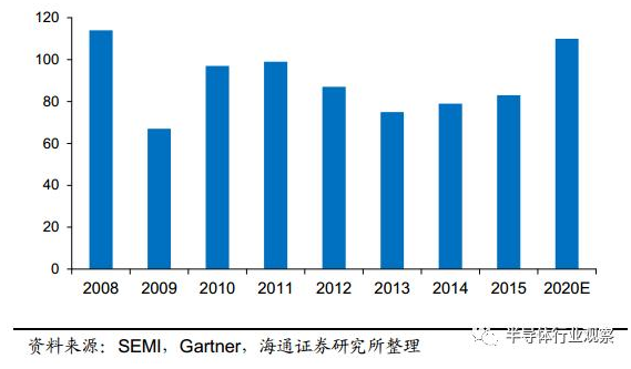
Global semiconductor wafer market size in 2008-2020 (US$100 million)
In terms of specific silicon wafers, the current mainstream silicon wafers are 300mm (12 inches), 200mm (8 inches) and 150mm (6 inches). Among them, 300mm silicon wafers have been market share more than 50% since 2009, and by 2015. The share has reached 78%, and it is expected that the demand for the wafer market will exceed 84% in 2020. 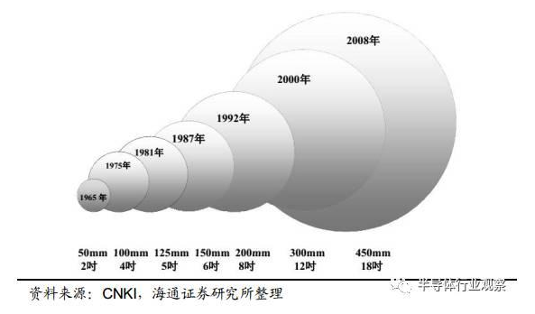
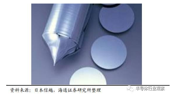
Monocrystalline silicon wafer main specification type
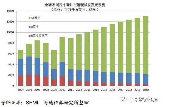
Global wafer market status and forecasts for 2005-2020 (millions of square inches)
In terms of silicon wafer selection, the reason why the shipment of 12-inch silicon wafers has grown rapidly in recent years is mainly due to the rapid growth of logic chips and memory memory chips such as CPU/GPU, most of which are manufactured by 12-inch wafers. . However, in addition to advanced chips such as CPU/GPU and Memory, more chips use 8-inch (200mm) wafers, such as automotive semiconductors, fingerprint recognition chips and camera CIS chips, and 2016 fingerprint identification chips and CIS chips. Benefiting from the significant increase in shipments in the smartphone market, automotive semiconductors have benefited from the rapid growth of automotive electronics, which is the main reason for the shortage of 8-inch wafers in 2016. At the same time, 450mm silicon wafers are expected to start mass production in around 2017. The first customers are only Intel. After a few years, the 450mm silicon wafer will follow the law and usher in a strong growth for a period of time. It is expected that the demand for silicon wafers will continue to grow. According to IC Insights, the 300mm wafer foundry will reach its peak around 2021, after which the market will be replenished with 450mm wafers, and 300mm will gradually decrease.
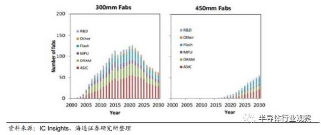
Global 300mm and 450mm wafer foundry forecasts
In terms of downstream applications of silicon wafers, according to a report released by IHS in December 2016, the global demand for semiconductor wafers in 2015 was 63.3 billion square centimeters, and the growth rate in 2016 is expected to be 3.8%. In 2015, the total consumption of smartphones and computers accounted for 41.23%, which is expected to decline in 2016. SSDs using NAND FLASH technology will achieve 33% growth, and other industries (industrial, automotive, home, gateway, etc.) ) will have a 5-10% increase.
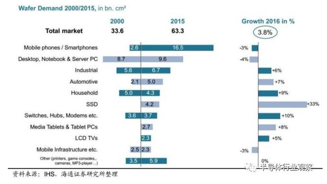
Global silicon demand situation - by downstream application market
Global semiconductor wafer industry competition pattern - giant monopoly
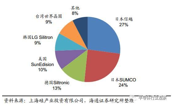
From a global perspective, silicon materials have a high monopoly. More than half of the world's semiconductor silicon materials are concentrated in Japan, especially as the size is larger and the purity is higher, the monopoly situation is more serious. In 2015, Shin-Etsu (Shin-Etsu) and Sumco, the top two global semiconductor wafer sales, are Japanese companies, and the third to tenth are: Siltronic in Germany, SunEdison in the US, LG Siltron in Korea, and Taiwan. Global Wafer, Soitec in France, Wafer Works in Taiwan, Okmetic in Finland, and Episil in Taiwan.
——The top ten semiconductor wafer companies in the world in 2015 (100 million US dollars)
Among them, Shin-Etsu's sales in 2015 exceeded US$2.1 billion, Sumco nearly US$2 billion, and the two Japanese companies together accounted for more than 50%. In Germany, Siltronic's sales in 2015 were nearly $1.05 billion. SunEdison Semiconductor, LG Siltron and Global Wafer had sales of between $700 million and $800 million, and the remaining sales were below $300 million. The group data shows that the monopoly of the silicon material industry is high, and the sales share of the top six wafer factories reaches 92%.
The top six semiconductor wafer factories in 2015 accounted for 92%
According to Gartner's data, the monopoly situation is even more pronounced in the 12-inch (300mm) large silicon wafers. The sales share of the top six semiconductor wafer factories in 2015 reached 97.8%.
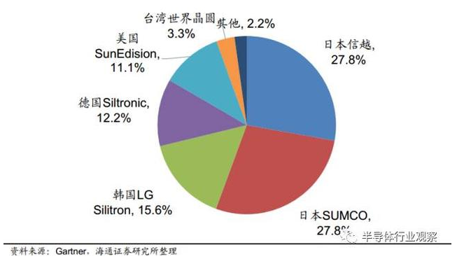
2015 300mm large wafer market share
The monopoly of the wafer industry is extremely high. In recent years, large companies have continued to achieve further market share through mutual integration. For example, Shin-Etsu acquired Hitachi's wafer company in 1999, and SUMCO was formed by the merger of Sumitomo, Mitsubishi Materials and Komatsu in 2002 and 2006. In September 2016, Taiwan's GlobalWafer acquired SunEdison Semiconductor for a total price of US$683 million, making the sixth-ranked Global Wafer a breakthrough in Siltronic as the world's third-largest supplier of semiconductor silicon materials. In May, Global Wafer also acquired the Danish wafer plant Topsil for 320 million yuan.
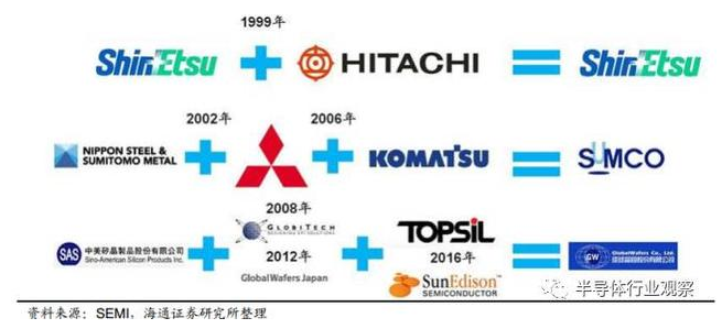
The top three semiconductor wafer suppliers are integrated by large-scale mergers and acquisitions
As the largest key material in the IC manufacturing industry, 300mm silicon wafers in mainland China have always relied on imports. The main reason is that there is no high-purity large-wafer technology for large-scale mass production of IC integrated circuits. The technical obstacles to making high-purity large silicon wafers are mainly the purity of silicon and the yield of large-sized silicon wafers. For advanced semiconductor wafers, the purity needs to reach 11 or more (ie, 99.999999999%), which is currently not possible in China. At the same time, large-size silicon wafers require high processing techniques such as chamfering and precision grinding. Have not yet mastered the high-yield technical capabilities.
Japan's Shin-Etsu wafers can be as pure as 11 or more
Who is the largest consumer of silicon wafers?
The main purpose of electronic grade silicon wafers is to process them into bare chips by supplying various foundry processes, and then package and test them into modular usable chips for application to different electronic terminals. Yuandai Factory is a major customer of electronic grade semiconductor wafers.
According to the statistics of IC Insights, an authoritative third-party organization, the scale of the global foundry industry was US$16.415 billion in 2004. In 2008 and 2009, due to the financial crisis, the industry scale grew negatively. In 2015, the market scale increased to 48.891 billion US dollars. The compound annual growth rate from 2004 to 2015 was 10.4%.
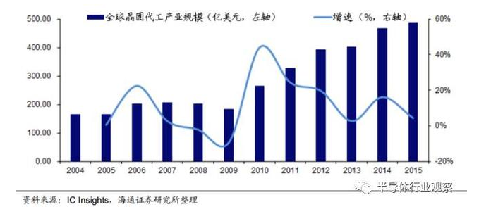
Global wafer foundry market size and growth rate from 2004 to 2015
In the past ten years, the global IC foundry business is dominated by five major manufacturers, namely TSMC, Taiwan UMC, Grofund (combined by AMD chip foundry and Chartered Semiconductor), Samsung and China SMIC. Internationally, the total share of the five companies is about 80%. 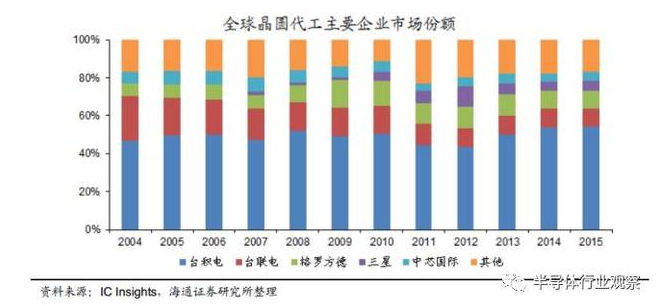
Market share of global foundry companies from 2004 to 2015
Among them, TSMC firmly holds the first position, and its share has remained at around 50% for a long time. In 2015, its market share was 54.3%, which is the leading distributor of global foundry. TSMC's revenue in 2015 was US$26.439 billion, up 5.5% year-on-year. It benefited from the introduction of 20nm process and 16nm FinFET process, meeting the needs of advanced application processors and baseband data processor chips. In terms of specific wafer production capacity, according to the “2016-2020 Global Wafer Capacity Report†released by IC Insights, the global electronic-grade wafer production capacity in 2015 was 16.35 million pieces/month (calculated as 200mm silicon wafer), which was year-on-year growth. 6%, if converted with 300mm silicon (300mm silicon area is 2.25 times 200mm silicon), it is 7.267 million pieces/month. This data includes IC integrated circuits and common semiconductor devices. Among them, Taiwan, South Korea and Japan ranked the top three, and mainland China's share was 9.7%.
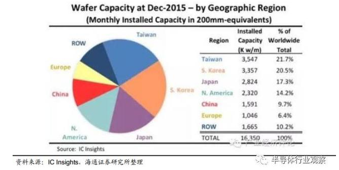
Global electronic grade semiconductor wafer capacity in December 2015 (calculated in 200mm silicon)
After surpassing Japan in 2011, Taiwan surpassed South Korea in 2015 and became the region with the largest capacity. Since December 2015, wafer production capacity in Taiwan has accounted for nearly 22% of the global total. In 2010, China overtook Europe for the first time in wafer production capacity. Japan has been a leader on wafers with a diameter of 6 inches or less. It currently produces low complexity process and commercial products or special components.
In terms of 8-inch wafers, Taiwan and Japan are leading. In the past few years, although many 8-inch fabs have been closed, Taiwan has not happened. This has helped Taiwan to become the No. 1 production area for 8-inch wafers since 2012. As Taiwan has become the region with the largest integrated circuit manufacturing capacity, it is expected that the region will continue to expand in 8-inch capacity in the next few years.
As for the 12-inch wafer, South Korea is ahead, followed by Taiwan. Taiwan lost its position as a leader in 12-inch wafers in 2013, a large part of which was due to the closure of the 12-inch fab by ProMOS, and partly because of Samsung Electronics and SK Hynix due to memory and flash Continued expansion of memory business needs.
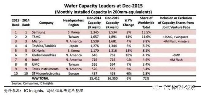
Wafer capacity of major global IC manufacturers in December 2015 (thousands/month)
As of December 2015, IC production capacity of the world's top ten manufacturers installed a total of 11.737 million pieces per month, wafers (in terms of 200mm silicon area), accounting for 72% of the world's total IC capacity, compared to 2014 In December, the monthly 108.85 million pieces increased by 7.8% year-on-year. According to the performance of various manufacturers, as of December 2015, Samsung is the semiconductor manufacturer with the highest installed wafer capacity, with a monthly capacity of 2.5 million 8-inch wafers, accounting for 15.5% of the global total capacity, of which the most produced. Is DRAM and FLASH flash memory;
The second largest is Taiwan's wafer foundry leader TSMC, with a monthly capacity of 1.9 million wafers, accounting for 11.6% of global production capacity. The memory capacity of memory giant Micron has continued to grow in recent years, mainly because of the acquisition. Production capacity of Elpida, Ruijing and Huaya Technology;
The fourth largest manufacturer is Toshiba, Japan, with a capacity of 1.3 million wafers per month. Its production capacity also includes flash memory capacity from the joint venture partner SanDisk;
The fifth largest manufacturer is also the memory industry - SK hynix in South Korea, the company's production capacity is also above 1.3 million wafers per month;
Intel's wafer capacity declined slightly in 2015 as the company's Fab 68 in Dalian, China, was temporarily suspended from the conversion of logic chip production to next-generation flash memory (3D NAND and XPoint memory).
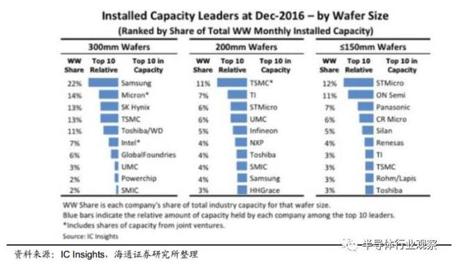
Forecast of production capacity of global foundry companies in December 2016
In terms of silicon wafer production capacity of different sizes of specific companies, according to IC Insights' report in December 16th, in the 12-inch wafer capacity ranking, Samsung won the world's first with 22%, followed by 14% of Micron, SK Hynix and TSMC ranked third with 13%. The fifth to tenth are Toshiba/WD (11%), Intel (7%), Grofonte (6%), UMC (3%), Powerchip (2%) and SMIC (2) %). Among them, Samsung, Micron, SK Hynix, Toshiba/WD mainly supply DRAM and NAND flash memory, TSMC, Grofund, UMC, Powerchip and SMIC are pure wafer foundries, mainly producing application processing. Logic devices such as devices. In the 8-inch wafer process, it is mainly based on pure-generation industrialists, analog/mixed-signal IC operators, and microcontroller manufacturers. Among the 8-inch fab capacity rankings, TSMC ranked first with 11%, Texas Instruments ranked second with 7%, and STMicro and UMC ranked third with 6%.
As for the 6-inch (in) and below wafer processes, the attributes of various industries are more diverse, including integrated components, automotive semiconductors and other products. Among the top ten players are integrated component manufacturers STMicroelectronics and Panasonic, automotive semiconductors ON Semiconductor and Renesas, and pure-wafer foundry TSMC.
As the current 18-inch fab development is still limited by excessive investment and technical barriers, it has been reduced to set targets.
As the 12-inch wafer process plays an increasingly important role in IC production, the number of ICs with 8-inch fabs has decreased from 76 in 2007 to 58 in 2016; however, with 12 The number of IC companies in the fabs also fell from 29 at the highest in 2008 to 23 in 2016. This is due to the increasing difficulty of the process, and the increasing technology and capital to the industry leader.
In summary, according to IC Insights, the global wafer monthly capacity in December 2014 and December 2015 was 1541 and 16.35 million pieces respectively (converted by 8 inch 200mm silicon wafer), equivalent to 12-inch wafer 685 and 7.27 million tablets. The memory chip manufacturers represented by Samsung, Micron, SK Hynix, Toshiba/WD and the pure wafer foundry represented by TSMC, Grofund, UMC, Powerchip and SMIC are the main production capacity. Contributors.
Komatsu Drive Parts,Komatsu Final Drive Parts,Komatsu Final Drive Assembly,Excavator Final Drive Parts
JINING SHANTE SONGZHENG CONSTRUCTION MACHINERY CO.LTD , https://www.stszcmparts.com